|
GLsun Science And Tech Co., Ltd
|

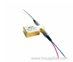
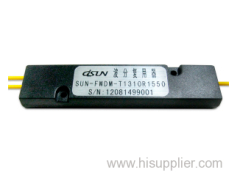
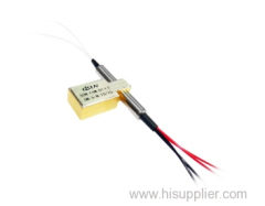
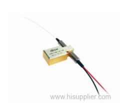
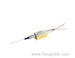
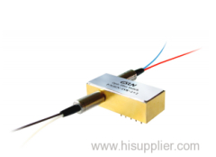
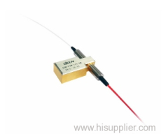
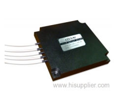
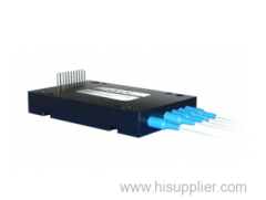
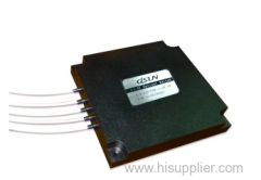
1×8T Optical Switch (Multi-channel Optical Switch)
| Payment Terms: | T/T,D/A,D/P |
| Place of Origin: | Guangxi, China (Mainland) |
|
|
|
| Add to My Favorites | |
| HiSupplier Escrow |
Product Detail
Features
@Wide Wavelength Range
@Low Crosstalk
@High Stability, High Reliability
@Epoxy-free on Optical Path
| Features | |
|
·Wide Wavelength Range ·Low Crosstalk ·High Stability, High Reliability ·Epoxy-free on Optical Path |
|
| Applications | |
|
·R&D in Laboratory ·System Monitoring ·OADM ·OXC |
|
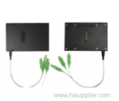
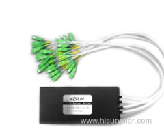
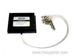
| SUN-FSW-1×8T Optical Switch is an ideal component for OADM,OXC,system monitoring and protection. With compact package, it can be easy to integrate into a high density optical communication system. | |
| Specifications | |
|
Parameters |
Unit |
SUN-FSW-1×8T |
|
|
Wavelength Range |
nm |
850±40 / 1300±40 |
1260 ~ 1650 |
|
Test Wavelength |
nm |
850 / 1300 |
1310 / 1550 |
|
Insertion Loss |
dB |
Typ: 1.3 Max: 1.5 |
|
|
Return Loss |
dB |
MM ≥ 30 SM ≥ 50 |
|
|
Crosstalk |
dB |
MM ≥ 35 SM ≥ 55 |
|
|
PDL |
dB |
≤0.15 |
|
|
WDL |
dB |
≤0.35 |
|
|
Repeatability |
dB |
≤±0.05 |
|
|
Durability |
Cycles |
≥ 10 Million |
|
|
Switching Time |
ms |
≤8 |
|
|
Optical Power |
mW |
≤500 |
|
|
Operating Temperature |
℃ |
-20 ~ +70 |
|
|
Storage Temperature |
℃ |
-40 ~ +85 |
|
|
Relative Humidity |
% |
5 ~ 95 |
|
|
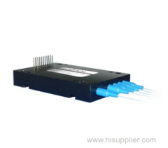
Dimension |
mm |
(L)86×(W)80×(H)16 ±0.2 |
|
|
Power Supply Requirement |
|
Parameters |
Min |
Typ |
Max |
Unit |
|
DC voltage supply ( 5V ) |
4.75 |
5 |
5.25 |
V |
|
DC voltage supply ( 3.3V ) |
3.14 |
3.3 |
3.45 |
V |
|
DC current supply ( 5V ) |
250 |
mA |
||
|
DC current supply ( 3.3V ) |
100 |
mA |
|
Pin Configurations |
|
Pin No. |
Signal Name |
I / O |
Description |
|
1 |
VCC1 |
Input |
5.0±5% VDC Switch Power Supply |
|
2 |
AGND |
Input |
Analog ground |
|
3 |
D0 |
Input |
LVTTL, Channel selection bit 0 |
|
4 |
D1 |
Input |
LVTTL, Channel selection bit 1 |
|
5 |
D2 |
Input |
LVTTL, Channel selection bit 2 |
|
6 |
Start |
Input |
LVTTL, Start strobe (Negative transition trigger) |
|
7 |
Ready |
Output |
LVTTL, Ready (High=Not ready, Low=Ready) |
|
8 |
Error |
Output |
LVTTL, Error (High=No error, Low=Error) |
|
9 |
DGND |
Input |
Digital (CMOS) ground |
|
10 |
VCC2 |
Input |
+3.3(3.14~3.45)V CMOS Power Supply (max. 100mA) |
|
11 |
NA |
||
|
12 |
NA |
||
|
13 |
S0 |
Output |
LVTTL, Switch status output bit 0 |
|
14 |
S1 |
Output |
LVTTL, Switch status output bit 1 |
|
15 |
S2 |
Output |
LVTTL, Switch status output bit 2 |
|
16 |
T0 |
Output |
LVTTL, Module type definition |
|
17 |
T1 |
Output |
LVTTL, Module type definition |
|
18 |
T2 |
Output |
LVTTL, Module type definition |
Related Search
Find more related products in following catalogs on Hisupplier.com
Company Info
GLsun Science And Tech Co., Ltd [China (Mainland)]
Business Type:Manufacturer
City: Guilin
Province/State: Guangxi
Country/Region: China (Mainland)